- 您现在的位置:买卖IC网 > Sheet目录443 > IRF530STRLPBF (Vishay Siliconix)MOSFET N-CH 100V 14A D2PAK
�� �
�
�IRF530S,� SiHF530S�
�Vishay� Siliconix�
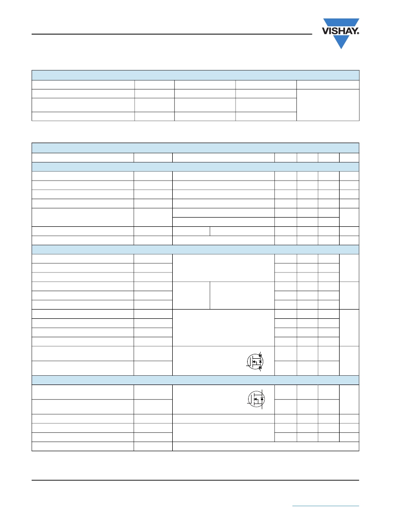
�THERMAL� RESISTANCE� RATINGS�
�PARAMETER�
�Maximum� Junction-to-Ambient�
�Maximum� Junction-to-Ambient�
�(PCB� Mount)� a�
�Maximum� Junction-to-Case� (Drain)�
�SYMBOL�
�R� thJA�
�R� thJA�
�R� thJC�
�TYP.�
�-�
�-�
�-�
�MAX.�
�62�
�40�
�1.7�
�UNIT�
�°C/W�
�Note�
�a.� When� mounted� on� 1"� square� PCB� (FR-4� or� G-10� material).�
�SPECIFICATIONS� T� J� =� 25� °C,� unless� otherwise� noted�
�PARAMETER�
�SYMBOL�
�TEST� CONDITIONS�
�MIN.�
�TYP.�
�MAX.�
�UNIT�
�Static�
�Drain-Source� Breakdown� Voltage�
�V� DS� Temperature� Coefficient�
�Gate-Source� Threshold� Voltage�
�Gate-Source� Leakage�
�Zero� Gate� Voltage� Drain� Current�
�V� DS�
�?� V� DS� /T� J�
�V� GS(th)�
�I� GSS�
�I� DSS�
�V� GS� =� 0,� I� D� =� 250� μA�
�Reference� to� 25� °C,� I� D� =� 1� mA�
�V� DS� =� V� GS� ,� I� D� =� 250� μA�
�V� GS� =� ±� 20� V�
�V� DS� =� 100� V,� V� GS� =� 0� V�
�V� DS� =� 80� V,� V� GS� =� 0� V,� T� J� =� 150� °C�
�100�
�-�
�2.0�
�-�
�-�
�-�
�-�
�0.12�
�-�
�-�
�-�
�-�
�-�
�-�
�4.0�
�±� 100�
�25�
�250�
�V�
�V/°C�
�V�
�nA�
�μA�
�Drain-Source� On-State� Resistance�
�R� DS(on)�
�V� GS� =� 10� V�
�I� D� =� 8.4� A� b�
�-�
�-�
�0.16�
�?�
�Forward� Transconductance�
�g� fs�
�V� DS� =� 50� V,� I� D� =� 8.4�
�A� b�
�5.1�
�-�
�-�
�S�
�Dynamic�
�Input� Capacitance�
�C� iss�
�V� GS� =� 0� V,�
�-�
�670�
�-�
�Output� Capacitance�
�Reverse� Transfer� Capacitance�
�Total� Gate� Charge�
�C� oss�
�C� rss�
�Q� g�
�V� DS� =� 25� V,�
�f� =� 1.0� MHz,� see� fig.� 5�
�-�
�-�
�-�
�250�
�60�
�-�
�-�
�-�
�26�
�pF�
�Gate-Source� Charge�
�Q� gs�
�V� GS� =� 10� V�
�I� D� =� 14� A,� V� DS� =� 80� V,�
�see� fig.� 6� and� 13� b�
�-�
�-�
�5.5�
�nC�
�Gate-Drain� Charge�
�Turn-On� Delay� Time�
�Q� gd�
�t� d(on)�
�-�
�-�
�-�
�10�
�11�
�-�
�Rise� Time�
�Turn-Off� Delay� Time�
�Fall� Time�
�t� r�
�t� d(off)�
�t� f�
�V� DD� =� 50� V,� I� D� =� 14� A,�
�R� g� =� 12� ?� ,� R� D� =� 3.6� ?� ,� see� fig.� 10� b�
�-�
�-�
�-�
�34�
�23�
�24�
�-�
�-�
�-�
�ns�
�Internal� Drain� Inductance�
�L� D�
�Between� lead,�
�6� mm� (0.25")� from�
�package� and� center� of�
�G�
�D�
�-�
�4.5�
�-�
�nH�
�Internal� Source� Inductance�
�L� S�
�die� contact�
�-�
�7.5�
�-�
�S�
�Drain-Source� Body� Diode� Characteristics�
�Continuous� Source-Drain� Diode� Current�
�Pulsed� Diode� Forward� Current� a�
�I� S�
�I� SM�
�MOSFET� symbol�
�showing� the�
�integral� reverse�
�p� -� n� junction� diode�
�G�
�D�
�S�
�-�
�-�
�-�
�-�
�14�
�56�
�A�
�Body� Diode� Voltage�
�Body� Diode� Reverse� Recovery� Time�
�Body� Diode� Reverse� Recovery� Charge�
�V� SD�
�t� rr�
�Q� rr�
�T� J� =� 25� °C,� I� S� =� 14� A,� V� GS� =� 0� V� b�
�T� J� =� 25� °C,� I� F� =� 14� A,� dI/dt� =� 100� A/μs� b�
�-�
�-�
�-�
�-�
�150�
�0.85�
�2.5�
�280�
�1.7�
�V�
�ns�
�μC�
�Forward� Turn-On� Time�
�t� on�
�Intrinsic� turn-on� time� is� negligible� (turn-on� is� dominated� by� L� S� and� L� D� )�
�Notes�
�a.� Repetitive� rating;� pulse� width� limited� by� maximum� junction� temperature� (see� fig.� 11).�
�b.� Pulse� width� ?� 300� μs;� duty� cycle� ?� 2� %.�
�www.vishay.com�
�2�
�Document� Number:� 91020�
�S11-1046-Rev.� C,� 30-May-11�
�This� document� is� subject� to� change� without� notice.�
�THE� PRODUCTS� DESCRIBED� HEREIN� AND� THIS� DOCUMENT� ARE� SUBJECT� TO� SPECIFIC� DISCLAIMERS,� SET� FORTH� AT� www.vishay.com/doc?91000�
�发布紧急采购,3分钟左右您将得到回复。
相关PDF资料
IRF540NL
MOSFET N-CH 100V 33A TO-262
IRF540STRR
MOSFET N-CH 100V 28A D2PAK
IRF5800TRPBF
MOSFET P-CH 30V 4A 6-TSOP
IRF5804TRPBF
MOSFET P-CH 40V 2.5A 6-TSOP
IRF6100PBF
MOSFET P-CH 20V 5.1A FLIPFET
IRF6100
MOSFET P-CH 20V 5.1A FLIP-FET
IRF6215L
MOSFET P-CH 150V 13A TO-262
IRF634B_FP001
MOSFET N-CH 250V 8.1A TO-220
相关代理商/技术参数
IRF530STRR
功能描述:MOSFET N-Chan 100V 14 Amp RoHS:否 制造商:STMicroelectronics 晶体管极性:N-Channel 汲极/源极击穿电压:650 V 闸/源击穿电压:25 V 漏极连续电流:130 A 电阻汲极/源极 RDS(导通):0.014 Ohms 配置:Single 最大工作温度: 安装风格:Through Hole 封装 / 箱体:Max247 封装:Tube
IRF530STRRPBF
功能描述:MOSFET N-Chan 100V 14 Amp RoHS:否 制造商:STMicroelectronics 晶体管极性:N-Channel 汲极/源极击穿电压:650 V 闸/源击穿电压:25 V 漏极连续电流:130 A 电阻汲极/源极 RDS(导通):0.014 Ohms 配置:Single 最大工作温度: 安装风格:Through Hole 封装 / 箱体:Max247 封装:Tube
IRF531
制造商:Rochester Electronics LLC 功能描述:- Bulk 制造商:Motorola 功能描述:IRF531 MOTOROLA S9G3A 制造商:Harris Corporation 功能描述:
IRF531FI
制造商:STMICROELECTRONICS 制造商全称:STMicroelectronics 功能描述:N - CHANNEL ENHANCEMENT MODE POWER MOS TRANSISTOR
IRF531R
制造商:HARRIS 制造商全称:HARRIS 功能描述:N-Channel Power MOSFETs Avalanche Energy Rated
IRF532
制造商:Rochester Electronics LLC 功能描述:- Bulk
IRF532FI
制造商:STMICROELECTRONICS 制造商全称:STMicroelectronics 功能描述:N - CHANNEL ENHANCEMENT MODE POWER MOS TRANSISTOR
IRF532R
制造商:HARRIS 制造商全称:HARRIS 功能描述:N-Channel Power MOSFETs Avalanche Energy Rated